
IBM Unveils 0.7-Nanometer Chip Tech With Big Efficiency Gains
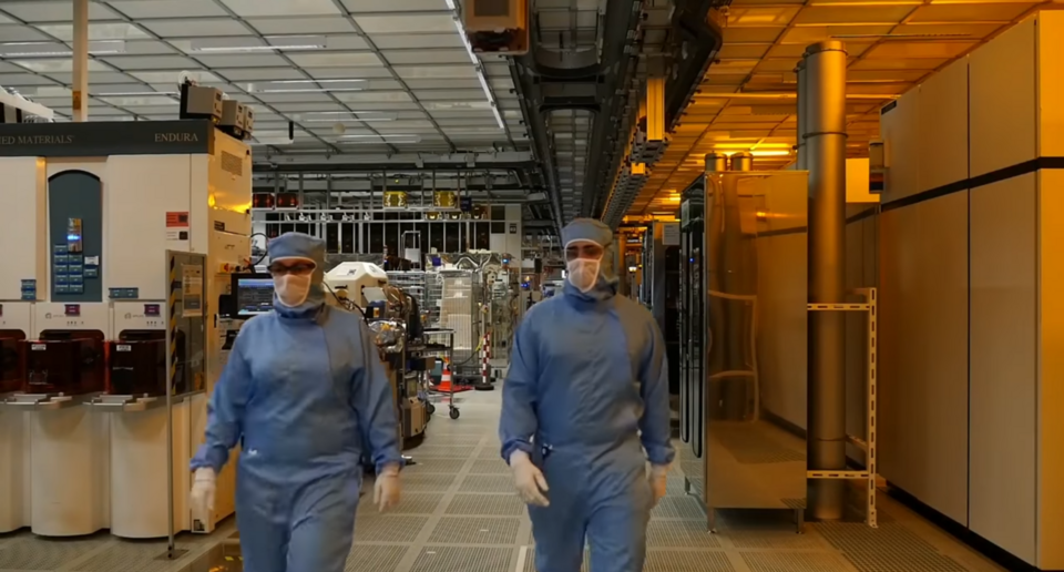
IBM announced a 0.7-nanometer-class semiconductor technology on Thursday, June 25, 2026, in Armonk, New York, promising big performance and power-efficiency gains.[1]
IBM said the design can deliver up to 50% higher performance or 70% greater energy efficiency compared with its existing 2-nanometer node.[1] The company described a prototype that uses a "nanostack" three-dimensional transistor architecture and places nearly 100 billion transistors on a fingernail-sized die.[1] IBM estimated a path to production of about five years but did not name a manufacturing partner.[1]
In May 2021, IBM announced a 2-nanometer chip that used nanosheet transistors to pack up to 50 billion transistors on a fingernail-sized chip. IBM Research first unveiled nanosheet architecture in 2015, and the new 0.7-nanometer prototype extends that lineage by stacking those sheets vertically into a nanostack to roughly double transistor density.
Global data center electricity use was about 415 terawatt-hours in 2024 and is projected to reach roughly 945 terawatt-hours by 2030, so gains in chip energy efficiency could matter at scale. Traders and industry observers flagged the efficiency claims, with social posts noting a premarket jump in IBM shares and questioning which foundry might commercialize the technology.
The mainstream summary does not address the significant implications of IBM's claims regarding energy efficiency in relation to the escalating electricity demands of global data centers. While it mentions that global data center electricity use was about 415 terawatt-hours in 2024, it omits the projection that this figure could nearly double to around 945 terawatt-hours by 2030, highlighting the urgency for energy-efficient technologies as AI workloads proliferate. This context emphasizes the potential impact of IBM's advancements, which could play a crucial role in mitigating the looming energy crisis in the tech sector. The summary also fails to mention that U.S. data centers alone consumed 176 TWh in 2023 and are projected to reach between 325 and 580 TWh by 2028, indicating a significant portion of the country's electricity demand is tied to data centers, further underscoring the importance of IBM's efficiency claims in a broader energy landscape.[2][3]
Show source details & analysis (1 source)
📊 Relevant Data
Global data center electricity consumption was approximately 415 TWh in 2024 (1.5% of world electricity use) and is projected to double to around 945 TWh by 2030 under the IEA base case.
Energy and AI — International Energy Agency
U.S. data centers consumed 176 TWh of electricity in 2023 (4.4% of total U.S. electricity) and are projected to reach 325-580 TWh by 2028 (6.7-12% of U.S. electricity).
2024 Report on U.S. Data Center Energy Use — U.S. Department of Energy / Lawrence Berkeley National Laboratory
📌 Key Facts
- On Thursday, June 25, 2026, IBM announced a 0.7-nanometer-class semiconductor technology in Armonk, New York.
- IBM says the design can offer up to 50% higher performance or 70% greater energy efficiency than its existing 2-nanometer node.
- The prototype chip uses a "nanostack" 3D transistor architecture and fits nearly 100 billion transistors on a fingernail-sized die, with IBM estimating a path to production in about five years.
📰 Source Timeline (1)
Follow how coverage of this story developed over time